
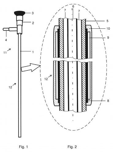
The invention relates to a device, to a system, and to a method for antimicrobial treatment during performance of operations in bodies, to a method for producing the device, and to a computer program. A device (11) is provided for antimicrobial treatment during performance of operations, in particular minimally invasive operations, in bodies. Said device comprises a main body (1) for partial introduction into a body and at least one plasma source (12) arranged in at least one portion of the main body (1). The plasma source (12) has at least one high-voltage electrode (9) which is covered at least partially and in particular completely with a dielectric (10) and is adapted to produce a plasma when an electric voltage is applied and in co-operation with a second electrode by means of dielectric barrier discharge.
Figures 1 and 2 of the Patent Specification
EP3429640 B1
1. A device (11) for antimicrobial treatment in the region of percutaneous accesses when performing interventions, in particular minimally invasive interven-tions, in bodies, having a base body (1) in the form of a shaft for partial insertion into a body, the device ( 11) being a device for endoscopy or a trocar,
wherein the device (11) further comprises at least one plasma source (12) arranged in at least one section of the basic body ( 1 ), wherein the plasma source (12) has at least one high-voltage electrode (9) which is at least partially and in particular completely covered with a dielectric (10) and which is configured to generate a plasma when an electrical voltage is applied and in cooperation with a second electrode by means of a dielectric barrier discharge, characterized in that in at least one section of the base body (1) the high-voltage electrode (9) and the dielectric (10) are arranged in layers around a cross-section of the base body (1 ), wherein a high-voltage-resistant insulating layer (8) is arranged between the base body (1) and the high-voltage electrode (9), wherein the dielectric (10) projects beyond the high-voltage electrode (9) on both sides in the axial direction, wherein the dielectric (10) contacts the insulating layer (8) in these portions and lies against the base body (1) beyond these portions.
| Field | Value | ||||||||||||||||||||||||||||||
|---|---|---|---|---|---|---|---|---|---|---|---|---|---|---|---|---|---|---|---|---|---|---|---|---|---|---|---|---|---|---|---|
| Patent Family |
| ||||||||||||||||||||||||||||||
| Applicant(s) | |||||||||||||||||||||||||||||||
| Inventors |
| Field | Value |
|---|---|
| Plasma Source Name | |
| Plasma Source Application | |
| Plasma Source Specification |